
PCB applications by market
Seven markets, seven sets of requirements. What follows is what a design in each sector normally has to specify — materials, constructions and documentation — written for the engineer who signs the drawing.
Three requirements decide the stack-up
A bare board has no application of its own. It inherits the environment it is assembled into — temperature, vibration, voltage, humidity, RF environment — and every one of those changes how the stack-up has to be built.
In practice three questions do most of the work. Mechanically: what does the board have to survive, and how is it mounted? Thermally: where does the heat go, and what is the path to the enclosure? Electrically: what voltage, what signal, and how tight does the impedance have to be? Answer those three and the construction usually follows — rigid, rigid-flex, HDI, metal-core or heavy copper.
The rest is specification discipline. Where a market works to a published standard — an IPC-A-600 workmanship class, a flammability rating, a RoHS or REACH material declaration — that standard belongs in the written specification and in the documentation package, so it can be reviewed before production starts rather than explained afterwards.
Every parameter quoted on this page is a starting point for the discussion, not a specification. Material, thickness, copper weight, tolerances and stack-up are confirmed against your drawing, your product's safety standard and your test plan before anything is built.
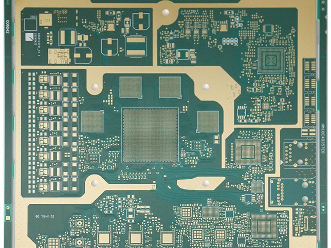
ECUs, battery management and body modules
A control unit next to an engine bay sees vibration, condensation cycling and a supply rail that moves while the starter turns. A body module in a tailgate sees temperature swings and little else. Both are described by the same drawing conventions and held to the same written material and documentation requirements.
Underneath the component, the solder joint is the weak point. Its life is governed by how far the board expands over temperature compared with how far the component does, which is why laminates with a higher glass transition temperature and a lower coefficient of thermal expansion are specified for under-hood and body electronics. Copper weight follows the current: motor drivers, contactor outputs and sensor returns carry far more than a signal trace, so the finished weight belongs on the drawing rather than in a quotation note.
At 48 V and above, spacing stops being a layout preference. Creepage and clearance across the board, around connectors and through slots are planned against the working voltage and the pollution degree, and press-in connectors need the affected inner layers copper-balanced because the pins move the pads they sit in during insertion. Lot-level traceability closes the loop — the laminate and foil lots behind a run, together with the electrical test results, let a field failure be traced back to a date and a lot.
- Thermal-cycling marginA high-Tg, low-CTE laminate keeps the strain between board and component small over repeated hot and cold cycles, and that strain is what the solder joint lives or dies by.
- Heavy copper on power pathsMotor drivers, contactor outputs and sensor returns carry more current than a signal board, so the finished copper weight is stated on the drawing instead of assumed.
- Creepage and clearanceAt 48 V and above, spacing across the board, around connectors and through slots is planned against the working voltage and the insulation requirement.
- Copper balance for press-fitPress-in pins move the pads they sit in during insertion, so the affected inner layers need copper balance requested explicitly in the drawing notes.
- Lot-level traceabilityThe laminate and foil lots behind a production run, with the electrical test results, let a field failure be traced back to a date and a lot.
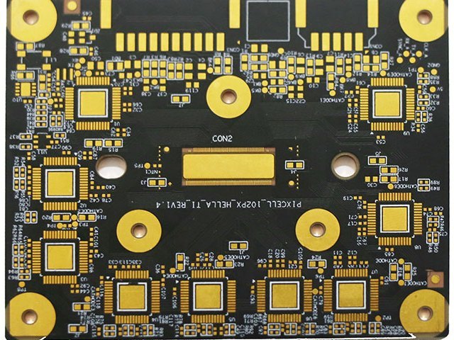
Inverters, chargers and LED drivers
Solar inverters, EV chargers, LED drivers, UPS modules and induction-heating controllers all push large currents through copper that is simultaneously dissipating heat.
Power electronics is a thermal problem that happens to be electrical. The heat source is small, the copper that carries the current is the same copper that has to move the heat away, and the enclosure is often sealed. That combination decides the construction: an aluminium or copper base spreads heat across the plane of the board instead of letting it pool under one device, heavy copper plating lowers the resistance and therefore the temperature rise along the path, and a via array connects the device to the opposite side when a metal core is not part of the design.
Mains-connected and DC-bus products carry a second layer of constraints. The safety standard the end product is built to sets the spacing at working voltage, and the isolation barrier between the primary and the secondary side is normally specified as a distance, a slot width and a defined insulation material. The finished board then has to carry the flammability rating and the material declarations that the same standard expects of the product it goes into.
The values above are indicative starting points for the discussion. The actual stack-up is agreed against your drawing and your product's safety standard before anything is ordered.
Routers, base stations and RF modules
Routers, base-station radios, RF modules, network switches and satellite terminals ask the same question in different words: will the signal still be the signal when it arrives?

At high data rates the answer depends on the dielectric and on the consistency of the stack-up rather than on the copper. A controlled-impedance design only works if the board is built to the stack-up the impedance calculation assumed, which is why a production release normally carries a stack-up table, a set of impedance coupons and a report showing the coupon measured inside the tolerance the design signed off. Where the loss budget is tight, the material grade is part of the specification rather than an upgrade applied later.
Above the impedance rules, most RF rework starts as a geometry problem: the length match between a pair, the via stub left behind when a signal changes layer, the connector that breaks the transmission line, the keep-out an antenna needs around itself. Each is a layout decision, and each only holds if the process repeats it — which is why board outline tolerance and finished copper tolerance are stated alongside the impedance values rather than treated as a second-hand detail.
Controlled impedance holds only if the finished board matches the stack-up the calculation assumed. We coupon-test the controlled layers and report the measured values with the shipment.

Audio, smart home and accessories
Audio products, smart-home controllers, accessories, toys and household appliances compete on cost per unit and on how quickly they reach a shelf.
The cost-down pressure is real, but the two faults that bring a consumer product back are soldering defects and connector failures, and both live in the board construction rather than in the feature list. The design question is how to reach the BOM target without spending the reliability margin that the margin was there to provide. Layer count is usually the largest single lever, because a board that is functionally two layers and is being built as four is paying for structure it does not use.
Where the constraint is shape rather than area, rigid-flex moves the connection off the board and into a flex, which removes a board-to-board connector and its solder joints along with it. Where the constraint is area, HDI with laser microvias keeps the same outline while freeing routing space behind it. Cosmetic requirements enter here as well: on a product where the board is visible, solder-mask colour, surface finish and silkscreen are specified as drawing items rather than as finishing preferences.
- Every layer earns its costEach layer adds material, process steps and a place for a defect to hide, so an unnecessary one is removed rather than paid for.
- Rigid-flex for 3D assemblyA flex hinge lets the board fold into the housing and takes the inter-board connector and its solder joints with it.
- HDI for thin form factorsAny-layer HDI with laser microvias reduces the board area needed for a given pin count, usually the binding constraint in a slim enclosure.
- Cosmetic finish and mask colourSolder-mask colour, surface finish and silkscreen legibility are specified as drawing items whenever the board is visible to the end user.
- Cost-down without yield lossA reduction that adds drilling complexity, thinner traces or a tighter finish trades margin for yield, so the two are reviewed together.

PLCs, robotics and surveillance
PLCs, servo drives, robotics controllers, instrumentation, IP cameras and access-control readers share one characteristic: they run continuously, and they are rarely attended when they fail.
A board that stops a production line costs more than the board that stopped it, so the specification in this market is built around continuous duty. The hardware sits near vibration sources, near heat and sometimes in the open, which pushes the operating temperature range, the mechanical robustness of the connectors and the environmental sealing of the assembly into the requirement list. Many of these products are conformal-coated for humidity and contamination, and coating adhesion depends on the surface finish, on the mask coverage and on the areas that are deliberately left bare.
The interfaces are the other half. Field wiring brings surge, transient and earth potential differences onto the board, so protection networks, isolation gaps and the creepage distances around them are planned into the layout at the same time as the signal routing. A board built for a clean laboratory bench and the same board built for a machine floor are not the same product, and the difference is written into the drawing and the inspection criteria.
- Continuous dutyUnattended equipment is specified with its thermal and reliability margin stated up front, because a field failure is slow to reach and expensive to correct.
- Extended temperature rangeIndustrial and outdoor equipment is specified across a wide temperature band, and the laminate, the solder mask and the components all have to stay inside it.
- Coating compatibilityCoating adhesion follows the surface finish and the mask coverage, so the areas left uncoated for connectors, switches and test points are defined on the drawing.
- Rugged connector footprintBoard-to-wire and board-to-board connectors are a mechanical as well as an electrical decision, and the footprint has to survive handling and vibration.
- Surge and isolation planningSurge, transient and isolation requirements drive the placement of the protection components, the position of the isolation gap and the barrier material used to create it.

Diagnostics and patient monitoring
Patient monitors, diagnostic analysers, imaging electronics, infusion pumps and laboratory instruments apply the discipline of precision electronics with two additions: the signals are small, and the device usually sits inside a regulated quality system.
Small signals set the layout rules. Analog front ends, mixed-signal converters and clocked digital sections have to be kept apart so that switching noise and ground currents do not end up inside the measurement path. That normally means a deliberate ground and return plan, reference planes placed under the sensitive nets, and a stack-up chosen for the impedance the design needs rather than for the lowest material cost. A dielectric that drifts between lots does not merely change a waveform — it changes the reading.
The regulated context adds a documentation requirement on top of the electrical one. Device makers working inside a formal quality system normally expect material declarations, the finished board's test results and lot traceability to be available for the device history file, and they fix the workmanship class, the coupon plan and the acceptance criteria before the first board is built rather than after a return.
- Low-noise analog layoutReference planes, guard traces and the separation of analog and digital return currents decide whether a small signal is readable at all.
- Mixed-signal separationSensitive analog sections are kept away from switching stages and fast digital clocks, with the ground structure planned in the layout instead of stitched in afterwards.
- Tight impedance controlImpedance-sensitive lines need a defined stack-up and a coupon-verified build, because a drifting dielectric moves the measurement and not only the waveform.
- Cleanliness and material recordsMaterial declarations, halogen-free specifications where they are called for and lot-level records are normally part of the purchase documentation.
- Traceability under design controlsWhere the device sits under design controls the board becomes a controlled item, so the drawing, the stack-up and the inspection results have to be retained and reviewable.
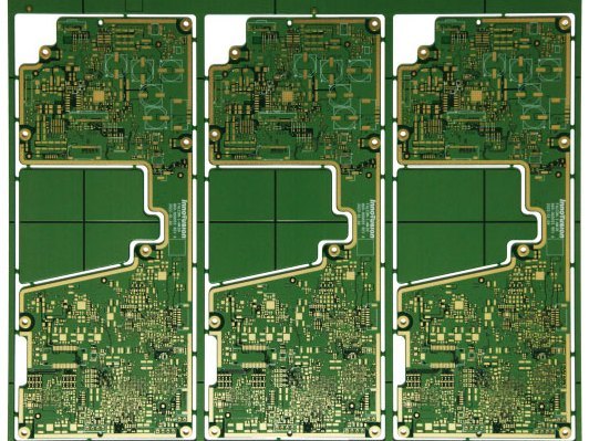
Phones, tablets and smartwatches
Phones, tablets, smartwatches, TWS earbuds and AR/VR headsets are area-constrained products in which the board has to fit around a battery, a display, an antenna and a set of mechanics.
Any-layer HDI is the usual answer to an area constraint. Laser microvias let the routing change layers without a through-drill, and a build-up structure with fine-pitch BGA lands lets the escape routing fit underneath the device. Where the problem is the shape of the product rather than its size, rigid-flex lets the circuit fold around the mechanics and removes a set of board-to-board connectors, which are both a cost item and a reliability item.
Wearables add a mechanical expectation that a desktop board does not have. The product is dropped, bent and twisted every day in a pocket, so the flex material, the bend radius and the transition region between the rigid and the flex area are specified as engineering values. A repeated bend is a fatigue problem: the copper and the adhesive in that transition carry the strain, and the geometry of the strain relief decides how many cycles it survives.
Both are stated as engineering values rather than left to the fabricator. They are confirmed against your drawing and your drop and flex test plan before the stack-up is fixed.
What to send with an application enquiry
Most delay in a first quotation comes from information that never arrived, not from information that was hard to find. If your product sits in one of the seven markets above, these are the items that let us quote against the real board instead of an approximation.
Send us the files, not a vague description
Gerbers, a stack-up, or just the question you are stuck on. We answer inquiries during Monday to Saturday, 9:00–18:30 (GMT+8).